
This is an old revision of the document!
Table of Contents
Reverse Engineering a NAND Flash Device Management Algorithm

Around June of 2012, I had gotten myself into a very bad habit. Instead of carrying my SD card in my camera, I left it sticking out of the side of my laptop, presumably intending to do something with the photos on it eventually. On my flight home from Boston, the predictable thing happened: as I got up out of my seat, the machine fell out of my lap, and as the machine hit the ground, the SD card hit first, and was destroyed.
I was otherwise ready to write off the data stored on that device, but something inside me just wasn't happy with that outcome. Before I pitched the SD card in the trash, I took a look at what remained – as far as I could tell, although the board was badly damaged, the storage IC itself was fully intact (although with a few bent pins).
The following is a description of how I went about reverse-engineering the on-flash format, and of the conclusions that I came to. My efforts over the course of about a month and a half of solid work – and a “long tail” of another five months or so – resulted in a full recovery of all pictures and videos that were stored on the SD card.
If you're just looking for the resources that go with this project, here are the pictures of the hardware, and here is the source code.
You can discuss this article on Hacker News.
Introduction
It is probably fitting to start with a motivation for why this problem is complex; doing data recovery from a mass-production SD card seems like it should be a trivial operation (especially given the interface that SD cards present), but as will become clear, it is not. From there, I will discuss the different parts of the problem in detail, both in terms of how they physically work, and in terms of what it means from the standpoint of a data recovery engineer.

I begin with a brief history of the field. In the past ten years, solid-state data storage has become increasingly complex. Although flash memory was originally commercialized in 1988, it only began taking off as consumer mass storage recently. In August of 2000, COMPAQ (and later, HP) began producing the iPAQ h3100/h3600 series of handheld computers, which had between 16 and 64MB of flash memory. This was approximately a standard capacity for the time period; the underlying technology of the flash device was called “NOR flash”, because of how the memory array was structured. NOR flash, in many regards, behaved like classic ROM or SRAM memories: it had a parallel bus of address pins, and it would return data on the bus I/O pins in a fixed amount of time. The only spanner in the works was that writes could only change bits that were previously ones to zeroes; in order to change a zero back to a one, a whole block of bits (generally, around 16 KBytes) had to be erased at once.
This was okay, though, and we learned to work around these issues. NOR flash had a limited erase life – perhaps only some millions of erases per block – so filesystems on the device generally needed to be specially designed to “wear-level” (i.e., scatter their writes around the device) in order to avoid burning an unusable hole in the flash array. Even still, it still appeared a lot like a block device that operating systems knew how to deal with; indeed, since it looked so much like SRAM, it was possible to boot from it on an embedded system, given appropriate connections of the bus pins.
Around 2005, however, NOR flash ran into something of a problem – it stopped scaling. As the flash arrays became larger, the decode logic began to occupy more of the cell space; further, NOR flash is only about 60% as efficient (in terms of bits per surface area) as its successor. To continue a Moore's Law-type expansion of bits per flash IC, flash manufacturers went to a technology called NAND flash. Unfortunately, as much as it sounds like the difference between NOR flash and NAND flash would be entirely internal to the array, it isn't: the external interface, and characteristics of the device, changed radically.
As easy as NOR flash is to work with, NAND flash is a pain. NOR flash has a parallel bus in which reads can be executed on a word-level; NAND flash is operated on with a small 8-bit wide bus in which commands are serialized, and then responses are streamed out after some delay. NOR flash has an amazing cycle life of millions of erases per block; modern NAND flashes may permit only tens of thousands, if that. NOR flash has small erase blocks of some kilobytes; NAND flash can have erase blocks of some megabytes. NOR flash allows arbitrary data to be written; NAND flash imposes constraints on correlating data between adjacent pages. Perhaps most distressingly of all, NOR flash guarantees that the system can read back the data that was written; NAND flash permits corruption of a percentage of bits.
In short, where NOR flash required simply a wear-leveling algorithm, modern NAND flash requires a full device-management algorithm. The basic premises of any NAND device-management algorithm are three pieces: data decorrelation (sometimes referred to as entropy distribution), error correction, and finally, wear-leveling. Oftentimes, the device management algorithms are built into controllers that emulate a simpler (block-like) interface; the Silicon Motion SM2683EN that was in my damaged card is marketed as a “all-in-one” SD-to-NAND controller.
Data extraction

Of course, none of the device-management information is relevant if the data can't be recovered from the flash IC itself. So, I started by building some hardware to extract the data. I had a Digilent Nexys-2 FPGA board lying around, which has a set of 0.1“ headers on it; those headers are good to around 20MHz, which means that with some care, I should be able to interface it directly with the NAND flash.
A bigger problem that I had facing me was that the NAND flash was physically damaged. The pins still had pads on them, ripped from the board; the pins were also bent. Additionally, the part was in a TSSOP package, which was too small for me to solder directly to. I first experimented with doing a “dead-bug” soldering style – soldering AWG 36 leads directly to each pin – but this proved ultimately too painful to carry out for the whole IC. Ultimately, I settled on using a Schmartboard; I sliced it in half, and allowed each side to self-align. This meant that I didn't have to worry about straightening both sides at the same time – as long as I got them each individually, I could get a functional breakout from the flash IC. (The curious reader might enjoy some photos of my various attempts to re-assemble the NAND flash.)
The next question was the mechanics of using the FPGA to transfer data back
to the host. I used Digilent's on-board EPP-like controller to communicate with the FPGA; ultimately, I
created a mostly-dumb state machine interface on the FPGA, which could be instructed to
perform a small number of tasks. It knew how to latch a command into the
FPGA, it knew how to latch data in and out of the FPGA, and it knew how to
wait for the flash to become ready – beyond that, everything was handled in
a wrapper library that I wrote on the host side. (Verilog source for this chunk of code, which I called ndfslave, is available; if you ever need some sample RTL to read for how to communicate with the Digilent EPP controller, this might be useful.)
To test that my interface was working correctly and use it, I wrote three tools:
id: Theidtool interrogated the flash's identification registers, and decoded all of the registers as best it was able. This was a basic diagnostic proving that both commands worked and data reads worked. (source: flash-det.c)iobert: IOBERT stands for “I/O Bit Error Rate Test”. Instead of simply reading the identification registers once, it spun in a tight loop repeatedly rereading them, and comparing them on each iteration. When I built the interface, the length of the wires (and lack of termination) concerned me, so I wanted to make sure that there weren't any timing or integrity marginality issues. I ran the BERT test overnight, transferring some 25GB, without error. (source: iobert.c)flash: This was the main driver; its purpose in life was to dump the flash device. Since the flash device is split into two chip-enables, it dumps each in sequence into their own files. With some optimizations, theflashtool peaked around 1.2 MByte/second – a far cry from the limits of either the NAND flash or the USB interface, but still sufficiently performant to dump both chip selects in about 6.5 hours. (source: flash.c)
One curious challenge was that no datasheet existed for the chip that I had. I used the closest available, but even that did not mention some important characteristics of the chip – for instance, it did not discuss the fact that there is an “address hole” between page 0x80000 and page 0xFFFFF, and that the rest of the data begins at 0x100000. (This comes from the fact that this flash IC is a “multi-level” flash chip, which means that each cell in the array stores three bits, not just one. The address hole exists, then, because three is not an even power of two...). The datasheet also does not mention that the chip has multiple chip-selects.
The end result of this phase was a pair of 12GiB files, flash.cs0 and flash.cs1, which contained the raw data from the NAND flash medium.
Unwhitening
Modern NAND flash devices have a bunch of difficult constraints to work with, but one that might not be obvious is that it matters what data you write to it! It is possible to construct some “worst case” data patterns that can result in data becoming more easily corrupted. As it turns out, the “worst case” patterns are often when the data we write is very similar to other data nearby; to solve this, then, a stage in writing data to NAND flash is to “scramble” it first.
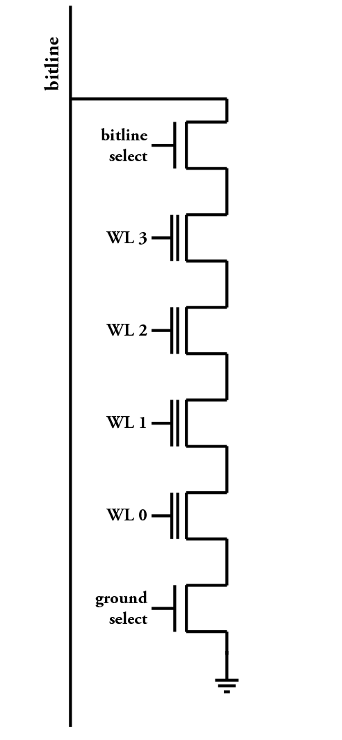
To understand how this can be, I've included an image to the right that shows a schematic of how the building blocks of NAND flash work internally (adapted from this drawing, from Wikipedia). This drawing shows one column of a NAND flash that has four pages; in total, four bits are represented here. To read from one page of flash, a charge is placed on the bitline, and then all of the wordlines (labeled 'WL') except for the one that we wish to sense are turned on. This means that charge can flow through the flash transistors that we're not trying to sense, and the one that we're trying to sense controls whether the charge stays on the bitline or whether it flows to ground. Then, some time later, we can sense whether that flash transistor was programmed or not by telling how much charge was left on the bit line. (This is a very simplified discussion, that may not make much sense without some background in the field. That's okay; this won't be on the final exam. The Wikipedia article on flash memory explains in some more detail, if you're interested.)
The problem with this is that the bypassed transistors (that is to say, the ones that we're skipping over – the ones that we're not sensing) are not perfect. Even though they are supposed to conduct when they are being bypassed, if they have been programmed, they might conduct slightly less well. If a few of the bits on that bitline have been programmed, that's not a problem; but if all of them except for the one that you're trying to read have been programmed, then it might take quite a lot longer for the bitline to become discharged, and the sense amp that reads the charge later could incorrectly read the transistor you're trying to sense as having been programmed.
This has only become a problem recently, as we've moved to more modern technologies. On larger processes, the effects that caused this to happen were apparently less likely; to compound the problem, multi-level flash chips, which use multiple voltage levels to encode multiple bits in a single transistor, require even more sensitivity in the sense amps. So, if other cells on the bitline are adding extra resistance, there no longer needs to be a flip all the way from one end to the other, but a small change in the middle can happen, which could still disrupt the read.
Even if you didn't understand the mechanics of it, what this means from the perspective of programming the device is that if many adjacent pages all have the same value, a page that has a differing value might be very hard to read, and might often flip to the “wrong” value when you try to read it. This affects each bit in the page individually, so if it happens to all of the bits, then even error correction will not be possible. The upshot of this is a new constraint on NAND flash: pages in the same block shouldn't have data that's excessively correlated.
The solution to this problem, then, is to add another step – I'll take the obvious name, “data decorrelation”. (Sometimes, other people call it “data scrambling”, “entropy distribution”, or “data whitening”.) The basic idea is to mix deterministic noise into the data on a per-page basis, and hope that the noise doesn't have the same pattern as the data that the user is trying to store. On flash, the data will look like garbage, so to get real data back out, you must then remove the noise – a process that I call “unwhitening”.
Mechanics
I started off without knowledge of the reason for scrambling the on-flash data, and began by looking for a one-byte XOR key that would find the FAT32 filesystem marker somewhere on the device. I did an exhaustive search of all possible one-byte XOR keys, while scanning the device for the FAT32 marker; one came up with a result, but not at a sensible offset, and no other plaintext that I would expect from the device (for instance, no DCIM or DSC0xxxxJPG). (I originally called this tool xor-me, but that tool eventually morphed into a generic tool to xor two files together.)
Since I wasn't recovering anything from a one-byte key, I wanted to know whether there was anything sensible to be recovered from an otherwise-short key. I figured that if there were real data around, the distribution of bytes would not be uniform, so I wrote a program that I called entropy to do a distribution analysis both on byte values and bits per byte. Irritatingly, I found that the distribution was pretty even, indicating that I was unlikely to find any real data around by simple methods.
Around this time, I was talking with Jeremy Brock, of A+ Perfect Computers. I was pasting him some samples of some pages on the device, and he recognized one of them as looking like an XOR key that he'd seen before. This was progress! I wrote a tool that looked for that pattern, matching on blocks in which it appears, and doing a probabilistic analysis on the rest of the block to figure out what bytes were likely to appear there (I reasoned that either zeroes or FFs were the most likely byte on the medium). Since the tool seemed to be looking for the known-pattern needle in the haystack of the image, I called it haystack-me.
It produced vaguely satisfactory output – I started to see directory structures – but some blocks didn't have the needle in them at all, and so I was still missing more than half of the medium. I was considering doing a more intelligent search, looking for common patterns (I didn't want to come up with patterns lost in the noise), but I decided to run an experiment first – I wanted to know if the most naïve thing possible could work. I wrote a tool to do a probabilistic analysis on a byte-by-byte basis in each row, without regard to every other byte in the row; from some of the results in haystack-me, I knew that the key repeated every 64 rows, so I picked the most common byte for each column in each row (mod 64). Since the algorithm was somewhat stupid, I called this tool dumb-me.
Both of these tools produced a “confidence” value for each byte in the extracted pattern, based on how probable the selected key byte was in relation to the second most-common byte. dumb-me produced satisfactory results with almost no further tweaking; it ended up being the method I chose to extract the key.
Once I had extracted the key, I ran the entire image through a new, revised xor-me, to produce a full flash image that had been unwhitened.
Future work
The probabilistic method for extracting a key, of course, kind of sucks. It's bad because it's not a sure thing (it could always be fooled by sufficiently strange data), but it's also bad because it's not how the flash controller does the job. The key that I extracted, I treated as an opaque blob – that is to say, a chunk of data that has no real relation, and nothing interesting used to generate it. That works okay for my applications, but it can't possibly be the way a tiny flash controller does this.
To understand why, it's important to look at the size of the key that I extracted – 512 KB per chip select. This is a completely unreasonable amount of memory to have in the controller; SRAM is very area-expensive, and only relatively large microcontrollers these days have that amount of memory. Those microcontrollers likely sell for some $7 a shot, primarily driven in cost by the die area for the SRAM, so it's not really possible to drive the price lower for that much SRAM in a different application. $7 would be up to half (if not more) of the bill-of-materials cost for this SD card; clearly, this is untenable.
I suspect that the key pattern is generated, instead, by a pseudo random number generator. The easiest such to implement in silicon is a LFSR – a Linear Feedback Shift Register. (LFSRs happen to be good for quite a lot of things, actually; a basic coding theory textbook should cover many of them, and Wikipedia's article isn't half bad, either.) Good future work for the unwhitening step, then, would be to reverse engineer the generating LFSR, and generalize that step to other flash controllers.
ECC recovery

Vendors manage to drive the cost of NAND flash lower by allowing the flash memory to be “imperfect”. At the scale at which these flash devices are produced, it's infeasible to expect a perfect yield – that is to say, every bit of every flash device fully functional – so allowing manufacture-time errors permits more of the NAND flash parts produced to be sold. Additionally, data errors come intrinsically with the scale of the device: as the physical size of each transistor becomes smaller, the number of electrons that can be trapped in the gate also becomes smaller, and so it takes even fewer electrons leaking in or out to cause a bit to be flipped.
All of these add up to the expectation of NAND flash being unreliable storage. Some NAND flash devices can have a bit error rate (BER) as high as 10-5 mid-way through their lifetime1), which requires powerful error correcting schemes to bring the expected BER down to a reasonable level.
Basics of ECC
At first, the concept of improving a bit error rate without adding an extra low-error storage medium may seem somewhat far-fetched. Given an unreliable storage mechanism, how can any meaningful data be reliably extracted? The answer comes in the form of error correction codes – ECC, for short. For the sake of clarity, I will introduce some of the basic concepts of ECC here; sadly, modern high-performance codes require a deep understanding of linear algebra (indeed, one that I do not have!), so it is infeasible – and somewhat out of scope – to go into great detail in this article.
The underlying premise of any ECC is the concept of a codeword – a chunk of data that conveys additional error correcting information, on top of the user-visible data (the “input word”) that it is meant to encode. Needless to say, the codeword is always larger than the input word; ECC schemes are sometimes described as being (m,n) codes, where there are m bits in each codeword, conveying n bits of data. There is a bijection between valid codewords and input words.

These codes derive their functioning from the idea of a Hamming distance (named after Richard Hamming, one of the pioneers of modern information theory). The Hamming distance between two strings of bits is the number of bits that would need to be corrupted in order for one to be changed to the other. (By way of example, consider the strings 8'b01100110 and 8'b01010110; the Hamming distance between these two strings is 2, because two bits would need to be corrupted in order to change the first to the second.) In an error correction code, all codewords have at least a certain Hamming distance from any other valid codeword; this minimum distance specifies the properties of the code.
Let's take some examples. A code with a minimum Hamming distance of 1 is no better than simply the input – there exists a single bit flip that could result in having another valid codeword, with no way of distinguishing that there was even an issue to begin with. A code with a minimum Hamming distance of 2 begins to offer some protection: if there is a single bit flip, the result no longer lands on a valid codeword, but it is not “closer” to either, so it's not possible to correct the error. A code with a minimum Hamming distance of 3 now allows us to correct a single error – if there is a single bit flip, the result is not any longer on a valid codeword, and it is also “closer” to one codeword than to any other, so it is possible to correct the error. However, since the minimum distance is 3, there exists at least one codeword for which two bit flips will result in silently “correcting” the error to the incorrect codeword; this scheme can also be described as a “single bit correction” system. By way of one more example, a minimum Hamming distance of 4 allows both the detection of two bits flipped, and the correction of one; this is a “Single Bit Correction, Double Bit Detection” (SECDED) scheme. (Such codes are very popular for volatile ECC memory with low bit rates.)
A simple ECC

To make this somewhat more concrete, I'll provide two examples of codes that are simple enough to construct and verify by hand. The first code is extremely simple, and has been used more or less since the dawn of time: for all values of n bits, we can produce a (n+1,n) code that has a minimum Hamming distance of 2 between valid codewords. The code works by taking all of the bits in the input word, and XORing them 2) together; then, take the single output bit from the XOR operation, and append it to the end of the input. This is called a “parity” code; the bit at the end is sometimes referred to as the parity bit.
You can see an example of this at right. In the first example, I've provided a valid codeword, with the parity check bit highlighted in blue. When I introduced a single bit error in the second example – placing the codeword at a Hamming distance of 1 to the original – a simple calculation will show that the parity bit no longer matches the data within, and so the code can detect that the codeword is incorrect. However, the code can detect only a single-bit error: in the third example, I have introduced only one more bit worth of error (for a total of two error bits), and the codeword once again appears to be valid. (This matches with our intuition for a minimum Hamming distance of 2; proof that 2 is in fact the minimum is left to the reader.)
Another simple ECC: row-column parity

The second code that I'll present is what I call a “row-column parity code”. In this version, I will give a (25,16) code: codewords are 25 bits long, and they decode to 16 bits of data. The code has a minimum Hamming distance of 4, which means that it can detect all two-bit errors, and correct all one-bit errors.
As you might expect from the name, this code is constructed by setting up a matrix, and operating on the rows and columns. To start, we will write the data word that we wish to encode – for this example, 1011 0100 0110 1111 – in four groups of four, and arrange the groups in a matrix. We will then compute nine parity operations: four for the rows, four for the columns, and one across all of the bits. (This is shown in the diagram at left.)

Although not terribly efficient, this “row-column” scheme provides a straightforward algorithm for decoding errors. At right, I show the same code, but with a single bit flipped; the bit that was flipped is highlighted in red. To decode, we recompute the parity bits on the received data portion, and compare them to the received parity bits. The bits that differ are called the error syndrome – to be specific, the syndrome refers to the codeword that is produces by XORing the received parity bits with the computed parity bits. To decode, we can go case-by-case on the error syndrome:
- If the syndrome is all zeroes – that is to say, the received parity bits perfectly match the computed parity bits – then there is nothing to do; we have received a correct codeword (or something indistinguishable from one).
- If the syndrome contains just one bit set – that is to say, only one parity bit differs – then there is a single bit error, but it is in the parity bits. The coded data is intact, and needs no correction.
- If the syndrome has exactly three bits set, and one is a row, one is a column, and one is the all-bits parity, then there is a single bit error in the coded word. The row and column whose parity bits mismatch point to the data bit that is in error; flip that bit, and then the error syndrome should be zero once again.
- If the syndrome is anything else, then there is an error of (at least) two bits, and we cannot correct it.
(It might not be immediately obvious why the all-bits parity bit is needed; I urge you to consider it carefully to understand what situations would cause this code to be unable to detect or correct an error without the addition of that bit.)
Linear codes
Before we put these codes aside, I wish to make one more observation about them. The codes above both share an important property: they are linear codes. Definitionally, a linear code is a code for which any two valid codewords can be added (XORed) together to produce another valid codeword. This has a handful of implications; for instance, if we consider the function ECC(d) to mean “create the parity bits associated with the data d, and return only those”, then we can derive the identity ECC(d1 XOR d2) = ECC(d1) XOR ECC(d2).
(This will become very important shortly, so make sure you understand why this is the case.)
NAND flash implementation
Of course, neither of the codes above are really “industrial-strength”. In order to be able to recover data from high-bit-error-rate devices like modern NAND flash, we need codes that are substantially more capable – and with along that capability comes a corresponding increase in encoding and decoding complexity. Most flash devices these days demand the capabilities of a class of codes called BCH codes (although LDPC is also becoming popular); these codes have sizes on the order of (1094,1024) or larger, and work on those amounts of bytes at a time, rather than bits! Such codes have the capability of correcting many many bad elements in a codeword, not just one or two; the downside, however, is that their foundations are rooted deep in the theory of linear algebra.
One thing to note is that even a BCH code with a codeword size of 1094 bytes is not capable of filling the quantum of storage in NAND flash (a “page”). On the NAND device that I worked with, the page size was as large as 8832 bytes – nominally, 8192 bytes of user data, and 640 bytes of “out-of-band” data. So, to figure out the page format on my SD card, I started by looking at a page that had content that I knew – in particular, a certain page in my data dump, once it was unwhitened, appeared to have bits of a directory structure in it. In this page, I saw the pattern:
| Start | End | Contents |
|---|---|---|
| 0 | 1023 | data |
| 1024 | 1093 | noise |
| ... | ||
| 6564 | 7587 | noise (zeroes) |
| 7588 | 7657 | noise (common) |
| 7658 | 8681 | noise (zeroes) |
| 8682 | 8751 | noise (common) |
| 8752 | 8777 | more different garbage |
| 8778 | 8832 | filled with 0xFF |
It seemed pretty obvious: the code that was being used was the (1094,1024) code that I described above. Seeing the same data – the zeroes at the end of the page – encoding to the same codeword gave me some hope, too. (If you'd like to follow along, my original notes discussing this are in notes/page-format, through about line 45.) The garbage at the end of the page wasn't immediately clear, but I figured that it was for block mapping, and decided that I'd come back to that later.
Decoding
Now that I knew where the codeword boundaries were, I was beginning to actually stand a chance of decoding the ECC! I started off by making some assumptions – I decided that it probably had to be a BCH code. Since my grounding in finite field theory is not quite strong enough to write a BCH encoder and decoder of my own, I grabbed the implementation from the Linux kernel, removed some of the kernelisms, and dropped it in as ecc/bch.c.
The next problem that I was about to face was that I wasn't sure what the whitening pattern for the ECC regions was. Although it was easy enough to guess by statistical analysis what the data regions would be, I didn't even know what the ECC regions were “supposed” to look like, so the same scheme as unwhitening the data region was unlikely to be fruitful. I pondered over this for a few days, and eventually came across a solution that I considered to be very elegant.
I discovered, in fact, that the ECC scheme didn't need any knowledge of whitening at all! As long as most pages were intact – which they were – I could come up with a scheme of correcting ECC errors without even running unwhitening. To come across this, it's helpful to think of a whitened data region as being represented by data_rawn = datan XOR d_whitener(n), and a whitened ECC region as being represented by ECC_rawn = ECCn XOR e_whitener(n). (We can leave the functions as opaque; and, of course, since XOR is commutative, the identities work the other way around as well.) From there, we can make the following transformations:
- Start with the basic ECC identity –
ECCn = ECC(datan)
- Next, unwrap into raw data –
ECC_rawn XOR e_whitener(n) = ECC(data_rawn XOR d_whitener(n))
- Next, hoist the whitener out of the ECC function, by the identities for linear codes given above –
ECC_rawn XOR e_whitener(n) = ECC(data_rawn) XOR ECC(d_whitener(n))
- Merge XOR functions that don't depend on the data –
ECC_rawn = ECC(data_rawn) XOR (ECC(d_whitener(n)) XOR e_whitener(n))
- And then finally make the XOR functions that don't depend on the data into a constant –
ECC_rawn = ECC(data_rawn) XOR kn
This is incredibly powerful! We have now reduced a function that wraps a whitener in complex and unpredictable ways into an XOR with a function of the block number. Since the whiteners that that function in turn depends on repeat, we can do a similar statistical analysis of ECC_rawn XOR ECC(data_rawn) in order to come up with an appropriate kn series. (My raw notes from the time live in notes/ecc.)
A curious property emerged when I did something like this. I found that the kns were all identical for every offset into the whitening pattern! This lends credence to the theory that the whitening pattern generator is somehow linked to the linear-feedback shift register internal to the BCH code.
Utilities
The tools for this were relatively straightforward, as these things go, but had a few hiccups. For instance, some pages were completely erased; attempting to correct them would not be terribly meaningful. Some pages had data, but none of it met with any sort of format expectations; I assumed that those were firmware blocks of some sort, and were not subject to either the same whitening scheme, or the same error correction scheme, as the rest of the device.
The largest complication was one that any expert in error correction codes would have foreseen by my explicit failure to mention it so far. One of the parameters that defines a BCH code is one that I haven't mentioned already – a “primitive polynomial” for the code. There can be many possible primitive polynomials for a given code size; in the Linux BCH implementation, the default primitive polynomial for a size-1024 code is 0x402b, but in the SD controller's implementation, the polynomial is 0x4443. If the polynomial differs, the error correcting code simply will not work at all on the stored data, and indeed, it didn't! This was a fairly baffling issue that took quite some staring before I figured out what was going on. Sadly, I didn't find a better mechanism than trial and error to find the appropriate polynomial; I found a list of polynomials of the correct size, and plugged in a few until I found one that worked. I suspect that it may be possible to figure this out deterministically with a modification of the BCH decode routine, but my knowledge of linear codes is not strong enough to implement such a thing myself.
The most interesting guts of the tool to decode this live in ecc/bch-me.c. My notes from above also showed how I extracted the ECC XOR constants.
Wear leveling
Even once we remove data interdependencies from a NAND flash device by whitening, and even after we make the device reliable to store data on by adding error correction, we have a final problem to deal with before we can treat it as a storage device similar to a hard drive.

The storage abstraction that we most readily concern ourselves with is that of a “linear block device”. What this means is that whenever we have a storage device that we would like to write to, we consider it as a collection of small blocks (sometimes, “sectors”) that can be individually addressed, and read and written independently of each other. In reality, of course, few devices actually behave this way: for instance, even hard drives divide their sectors up among drive heads, cylinders, and then sectors along the cylinders. Since it would be impractical for storage users to have to know the internals of each hard drive they access, hard drives since 1992-ish have implemented a scheme called 'Logical Block Access', in which the drive simply maps each sector on the disk to a single number identifying it.
This scheme worked well for early flash drives, too. The first generations of CompactFlash drives presented an interface in which flash blocks were mapped, more or less, one-to-one with the sectors that they presented to the host interface; when the host needed to do a write to a sector that already had data on it, the drive would erase the entire surrounding block, and then rewrite it with the new data. For small drives that saw infrequent (or otherwise linear) write traffic, this was not a substantial issue. However, as flash drives took greater popularity, demand for higher capacity grew, and there came to be a new breadth of use cases.
One of the reasons why older CompactFlash drives could get away with such a simple scheme was that they had relatively large write endurance (and were relatively slow). Every time a flash memory sector is erased, it sustains a small amount of damage; the process of pulling electrons off of the floating gate is not perfect, and electrons can sometimes be trapped in the gate oxide, resulting in a reduced voltage margin between bits that read as 0 and bits that read as 1.

These early devices could endure as many as a million erase cycles, since they were large enough that the available read margin was already quite large. As flash continued to shrink, the write endurance has also been shrinking; it is not uncommon to see quoted cycle lifetimes for NAND flash on the order of five thousand cycles, and new NAND flash may be rated for fewer than one thousand! Exposing these properties directly to the host system would make for storage media with an unacceptably short lifespan.
Additionally, as flash devies have grown, the minimum write sizes – and erase sizes – have also grown. Early NOR flash devices had erase block sizes of 32 Kbytes or smaller; on the NAND flash device that I used, the minimum write size is 8 Kbytes, and the erase size is a megabyte! In early CompactFlash media, it was plausible to erase the region around a sector that was being written, and rewrite it all, since the required buffer was so small, and the time taken was so low; on modern flash devices, it is increasingly implausible to erase an entire region when it is time to update a small portion of it. The need to erase before writing, then, is another property that a host system must be isolated from.
To deal with these problems and provide a more usable interface for host software, a collection of algorithms called “flash translation layers” have been developed. These algorithms are sometimes also called wear-leveling algorithms, since one of their purposes is to make sure that the entire surface of the flash device is written evenly. In order to extract the data from the error-corrected, unwhitened data dump, the final step is to reverse engineer the flash translation layer.
Solution space
Just as deep as is the history of flash translation layers, so is the solution space: over the years, as the requirements for a FTL have changed, the implementations of varied widely in how they work. One of the problems that a flash translation layer solves – the lookup from a virtual address to a physical location on disk – closely parallels the problem that a filesystem for a linear storage medium solves (that is to say, the lookup from a name to a physical location); the reader who is well-versed in filesystem technology, then, may find many similarities. I divide the classes of flash translation layers that I know of into two major groups: linear forward mapping systems, and log-structured systems.
The premise behind a linear forward mapping is that there exists a table somewhere that provides a mapping from every linear address to its physical address on the medium. The differentiating factors between these schemes are in how the table is stored: some, for instance, may store in a write-many non-volatile RAM, while others store directly on the flash itself. The 1:1 mapping that I described previously is the degenerate case of a linear forward mapping: the physical address can always be directly computed from the virtual address by a simple mathematical function.

One readily-apparent scheme for a linear forward mapping is to write a table to the flash medium that contains the current location of every block on the system. Whenever a block is remapped, the table is rewritten to the medium. In this algorithm, lookups are extremely performant: it takes only one read from the table to determine where any given virtual address is stored on the device, and oftentimes, the table is small enough to be cached into a controller's memory. However, the downside to such a simplistic algorithm is obvious: although hot-spots can be shifted away from the actual device data, the load is shifted onto the storage used for the metadata! (To borrow a turn of phrase, “quis wearleveliet ipsos wearleveles?”)
There exist variations on the linear mapping scheme, but before entering those, I would like to turn my attention briefly to its polar opposite: the log-structured filesystem. If a linear forward mapping writes all metadata to one location on the medium, the opposite must be to write it all over the medium – and that is precisely how log-structured filesystems work! One of the classic examples that is still in use on some systems today is the Journaling Flash Filesystem, Version 2, better known as JFFS2.
The general principle behind a pure log-structured filesystem is that data can be written to any “available” block on the medium, but that when they are written, they are written only once. If a datum needs to be modified, then a new version of the datum is written elsewhere on the medium, and and the old version remains in place until the storage is needed. (The cleaning process is called “garbage collection”.) The downside of this is that it can be quite expensive to read any given block, and that the mount procedure can take a long time: in order to determine where any given datum is, it may be necessary to scan the metadata of every block in the entire filesystem! In some regards, it can be said that a log-structured filesystem is reverse-mapped, in that the datum must be read to know where in the logical space it belongs.
The concept of a purely log-structured filesystem fell into disregard for some time, but is now making an interesting resurgence. The ZFS filesystem originally developed by Sun Microsystems uses a similar strategy, even though it primarily operates on media that are rewrite-tolerant; instead of aiming for wear-leveling, however, the advantage that ZFS gains is that it becomes resilient to power transients during writes. ZFS works by building a metadata tree, and updating all nodes above a block each time the location of a block is updated; although this creates additional disk traffic, it also ensures that no unnecessary blocks need to be scanned to find the latest version of a datum. (I am told that NetApp's Write-Anywhere File Layout, or WAFL, filesystem operates similarly, but I do not have direct experience with it.)
In reality, few systems are purely forward-mapped or are purely log-structured. It is generally to be expcted that any modern implementation will be a hybrid of the two architectures: for instance, long-stable data may be forward-mapped, whereas data that is rapidly changing may be log-structured. (A special case of this system is called journaling, where most data are forward-mapped, but recent data that needs to find space allocated for it is written to a small “journal” before it is committed to its final location.)
Initial experimentation
My goal, then, was to investigate the locations of known data on disk, and begin piecing together a mapping. Jeremy Brock, previously mentioned in this article, at one point noted that the out-of-band data in each block contains a reverse-map entry, but that I could expect to see duplicate block entries.
I used some known data to begin investigating what these sectors and blocks could possibly map to. I began searching through the image for volume header data (looking for the name of the drive in order to find it), and then as well for the FAT. Once I had read the volume header, I understood where logical sectors of the FAT needed to be; since most data on the original volume were contiguous, it was generally trivial to tell where any given FAT sector should live.
I found that the out-of-band data seemed to have two bytes in it that could
reasonably be a counter: bytes 2 and 3, which early in the filesystem were
ff ff and ff fe, seemed to look like an inversion of the block number!
This became important later; I began writing an initial tool to piece the
filesystem together based on this.
Given that the flash chip is split up into two virtual “chip select”s, I needed to know if blocks were interleaved. Looking at the first FAT entry I found, at block offset 0 from a FAT block, and chip select offset 0, I noticed that two adjacent pages were did not seem to go in order: there was a discontinuity of 3 pages' worth between each page. Eventually, I determined that this flash controller interleaved both by page within a chip select, and by chip select: for any given block, pages would be written in sequence to CS0+0x00, CS0+0x80, CS1+0x00, CS1+0x80, CS0+0x01, CS0+0x81, and so on.
Once I had a basic understanding, I began to write tools to extract data.
My first tool was called list-blocks, which pulled a confidence estimate out
of the chip for which reverse mappings were the most likely for any block
(by averaging across all of the out-of-band data in the block), and it also
provided a confidence estimate for each block in the forward mapping that it
generated as to how much data was found within it.
list-blocks produced an output file that was suitable for consumption by
another tool lofile: lofile behaved as a FUSE filesystem that
exported a single large (16GB) file. I then used Linux's lotools to set up a
loopback block device, so I could attempt to mount the filesystem or run
filesystem integrity checks.
The first attempts were inspiring, but not hugely promising. dosfsck,
when initially invoked before I understood the interleaving, reported
wide-scale garbage on the system: directories were full of noise, and the
FAT had lots and lots of garbage in it. Still, the general theory was
beginning to work! Blocks were falling into the right place, and *some* of
them were even correct. Once I corrected the interleaving, vast portions of
the filesystem became accessible.
Unfortunately for me, now that the easy problems were solved, the hard
problems remained. By that point, all directories were accessible, and
probably 98% of the data was as well, but dosfsck still complained of
somewhat large regions of empty FAT entries. Files on disk that were
expected to be of a certain size would simply have zeroes in the middle of
their FAT.
Sector updates
I continued down this path, and moved into an exploratory phase that my
notes refer to as the “bad-fat” phase. (Indeed, my raw notes from this time live in notes/bad-fat.) As usual, I went first by collecting
data, and wrote some tools to do this: command-word-by-block and
command-word-all-blocks did statistical analysis on the other metadata
stored in the OOB area, looking for patterns in what I suspected to be a
“command word” describing what each block's function was. Additionally,
unreferenced-pages computed a list of all blocks that were not in use by
the computed forward-table, in the hopes of finding either a firmware or an
on-disk forward lookup table. Unfortunately, none of these seemed to pan
out.
Failing these, I fell back on a more brutish approach. I knew that the FAT
sectors had to be on the medium somewhere, but I didn't know where.
Having no luck finding a forward mapping, I began searching for reverse
mappings for bad FAT entries by hand, and began developing a tool I called
patchsec. patchsec took a block that was known to have patch data
in it (that I had found by hand), and took a “vote” on each page within as
to which logical page was the most likely for it to correspond to. (Since
the FAT is mostly linear on a photo and video storage device, this sort of
statistical analysis became trivial.) Once it had high enough confidence for
any given page, it emitted a “patch list” of where reads should be
redirected to. (At some point, I referred to these small update mode as
“sector updates”, as opposed to a whole-block update; even though the
updates really work on a page granularity, some code will still reference
sector updates.)
I began updating lofile to support sector update lists, and eventually
set it up to take a configuration file of its own. As I continued to work,
lofile was a good start for experimentation, and was valuable for
invoking dosfsck, but the overhead of mounting and unmounting a loopback
device every time I needed to make a small change to the source distinctly
tempered progress (and, arguably, gave me a bad temper, too!).
Additionally, FUSE does not work on Mac OS X, and I was finding myself
spending more time doing development on my laptop, or otherwise somewhere I
couldn't shell to my Linux system. So, I split the lofile code out into
the FUSE front-end and the dumpio back-end library, and began writing a
tool I called fat.
fat was a very simple tool, built to be conceptually similar to tar;
it reused a FAT filesystem driver that I wrote for VirtexSquared, and
extended it with FAT32 support and with long file-name support.
Additionally, fat had support for working around holes in my recovery:
if it found implausible behavior in the primary FAT, instead of returning a
damaged file, it would attempt to read from the secondary FAT. This saved
me a fair bit of work.
Results
The fat tool allowed me, at long last, to effect a full recovery of all
of the data on my storage device! At this point, I was rather disheartened
by the need to use what felt like an excessively brute-force approach to
find data on the medium, but the triumph of having recovered my data seemed
to outweigh the questionable means by which I achieved it.
This leaves plenty of opportunity available for future work. For one, a blind reverse engineering approach may be valuable: there is still plenty of data on the volume, and it would be interesting to continue to undertake statistical analysis to determine what controls where it belongs. For another, it may be possible to find a controller firmware image on the device somewhere; this would be the “holy grail”, and would allow a true understanding of how the device operates. Documentation for the device indicates that it may contain an 8051 microcontroller.
Conclusions

In this article, I have described the full recovery of data from an SD card that sustained extensive physical damage. I have described the process of physically connecting to the flash medium; of electrically interfacing with it; of removing the “whitening” from the data; of repairing corrupted data using the ECC information on disk; and of translating linear addresses into physical addresses as controlled by a flash translation layer.
I hope that you have found this work inspiring in some way. I wrote this article because I was dismayed to find that much of the information that exists about recovering data from solid-state media is “hidden” away in the depths of some closed-source extraction tools; I hope that in publishing this, I have helped to democratize this understanding in some way.
In this article, I hoped also to convey one of the lessons that I learned from this effort: in short, “impossible isn't”. When conventional wisdom indicates that a device is unrecoverable, it is often the case that with sufficient effort, it is not just possible but reasonable to effect a full recovery of all of one's data.
This article is the culmination of six months of software programming, and nearly two years of on-and-off writing. I solicit your feedback. If you found this useful, or have information to contribute, please do not hesitate to get in touch with me. I look forward to hearing from you!
You can discuss this article on Hacker News.
1)
See, for instance, http://www.snia.org/sites/default/files/SSSI_NAND_Reliability_White_Paper_0.pdf – there are other remarkable things there, such as a 100-fold increase in bit error rate just by executing read cycles!
2)
Recall that XOR is defined as: 0 XOR 0 = 0; 0 XOR 1 = 1; 1 XOR 0 = 1; 1 XOR 1 = 0