
NOTE FROM THE FUTURE, September 2025: When the winding wire on the inductor on the boost converter is thicker than the wire for the input, this is a good indication that you may have no idea what you are doing. I wonder what I will think about my current designs in 2038.
The power factor correction stage for SSTC2 was based on Texas Instruments's UCC28019 integrated PFC controller. (For the rationale behind the use of a PFC circuit, see the main page for SSTC2.) Much of the PFC circuit is what one might expect, but for the sake of completeness in documentation, this page contains our implementation notes. Included also are schematics, for one who may wish to replicate this build, and overall lessons learned in designing the system.
The PFC circuit's design parameters were for a target output power of 1.5kW, a target output voltage of 350V, and a target input range of 100~240V. We used, as mentioned, around 60 turns of 10 AWG flexible-stranded wire wrapped around a Micrometals T400-34D toroid; for the input capacitor, we chose ten 0.1µF ceramics in parallel, and for the output, we placed a 0.1µF ceramic near the diode to eat up the switching hash, and a 2-series-2-parallel network of film capacitors (for a total capacitance of 1.2µF) a ways further away to absorb the overall 60kHz ripple.

Our design generally was done by the book. For a switching MOSFET, we used a Fairchild FCA36N60NF, and for the boost rectifier, we used a Fairchild RURP3060, which are both certainly well sized for what we intended to do. (The FET is rated for 600V and 36A, whereas we will be loading it at maximum with 400V or so, and an RMS current of 12A; the diode is similarly oversized.)
The points of innovation, then, were primarily in assembly. The UCC28019's sample layout is designed for circuits handling somewhat lower power, and is best done with a printed circuit board; for ease of assembly and prototyping, though, we experimented with ways of putting this circuit together that didn't involve sending anything off to a board house.
Basic operating principles
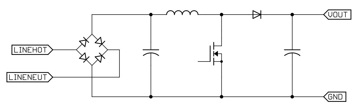
Before diving too deeply into how we built our system, I should provide a quick overview for those readers unfamiliar with the basic operation of a power factor correction circuit. (Those who know already should feel free to skip this section.) Power factor, for those unfamiliar, is how much the current from the power mains is in phase with the voltage; since the voltage coming from the mains is sinusoidal, ideally the current would also be sinusoidal, proportional to the voltage. Circuits that simply charge a capacitor from the mains through a diode, however, have large current peaks as the input voltage transitions above where the output voltage has sagged to, and no current the rest of the time; so, those circuits have relatively poor power factor.
The power factor correction circuit is designed to avoid that by "forcing" current into the output throughout the line cycle. It does that through the basic mechanism of a boost converter -- a switch-mode power supply that converts a lower input voltage into a higher one. In the schematic at right, the switch periodically closes, causing current to ramp up through the inductor; once energy is stored in the inductor, the switch opens, and current flows through the diode into the load. The control circuit detects both the input voltage and the output voltage, and modulates the switch waveform to keep the output voltage at a reasonable level, and to keep the input current waveform in phase with the input voltage waveform.
For more on switch-mode power supplies, I suggest reading through the excellent smpstech.com, in addition to your favorite textbook (or your favorite online encyclopedia, as it may turn out). Dave Jones's EEVblog has an episode on power factor correction using the MC34262, which looks like a part designed for somewhat lower power.

Attempt 1: Red wires
The first iteration put the control logic on its own piece of perfboard, attaching the power components through something analogous to a Berg strip. This, actually, turned out to work pretty well; it increased maintainability and assemblability, since it meant that the thick wire portions were not inextricably linked to part that required many fiddle little connections between all the passives in the world.
To connect the power components, we first got a nicely sized heatsink from Halted Surplus, and screwed the parts in, using silpads and shoulder washers to isolate them all. We then placed some Kapton tape under the terminals, and used the left over 10ga wire from the boost inductor to connect each of the parts up.
From this, a few things were discovered. First, 10ga wire, even in extremely finely stranded form, is a bear to solder. It required feeding extreme amounts of solder (and extreme amounts of heat!) into it in order for the solder to permeate through, and connecting multiple pieces of 10ga on the same terminal (for instance, on the bridge rectifier) proved to be a pain. This vastly decreased the maintainability of the system in the event of a FET failure, and although the wire looked OK, the solder connections themselves did not always look great (often they looked 'cold', or otherwise did not have the solder bonding all of the strands together).
Second, having long lengths of wire causes undesirable electrical effects. The wires must have added a fair bit of inductance to the system, because quite a bit less than expected of the switching hash got eaten up by the capacitors. Further, they behaved as excellent antennae; the PFC circuit had very severe EMI problems, causing every active circuit nearby it to misbehave in new and exciting ways. (For instance, the connected bias power supply for the UCC28019 gave wildly swinging readings for voltage and current output on its front panel display; the connected El-Cheapo DMM on the output lit up the 'check battery' and 'I am now measuring frequency instead of voltage' indicators, and proceeded to spew random numerals on the screen; and the isolated (!) oscilloscope proceeded to trigger at any trigger setting even when no (!!!) inputs were connected.)
Beyond that, though, the circuit passed initial validation. It happily output 80W into a test load, and when the inputs and outputs had ferrites attached to them, circuits nearby no longer totally lost their minds. It made a concerning buzzing on startup (more on that later), but beyond the remaining EMI and component stress issues, it seemed to work.

Attempt 2: Dremel board
We decided in the end that the "red-wire" implementation wouldn't really be suitable; some issues that originally looked like instability (the gate waveform varying -- it turned out that that was the PFC doing its normal thing... hurr...) tipped us over the edge to finding a better way to attach the components together. Steve Conner suggested that a lot of the switching hash was from lead inductance, and that we should do our best to decouple the diode current loop (and to keep that loop as short as possible). In the shower, I thought of an elegant solution leveraging what we had the ability to do at home, and I went to Halted again that afternoon; I returned with some copper clad, and some new engraving bits for the Dremel.
I cut holes in the copper clad for where the leads looked like they should go, and then bent them up and poked them through the holes. I also cut holes for the screws in the parts, so if any part failed, I could simply unscrew everything, lift the board up, and change out the part. After some careful trial and error, I got all of the parts lined up; after poking them through, I used the engraving bit to make "anti-traces" around each circuit node.
This new layout has a few salient features. First, the output capacitance is much closer; second, the input capacitance is, too! Actually, basically everything is much closer, and that's a good thing, since it means that the diode current loop should be much smaller. The piece of copper clad is also held fairly well in place by a bunch of leads that are not very willing to bend; the effect is a piece of copper clad hovering some .5" off of a heat sink, making a very nice tight "power brick" package. I also added a 0.1µF ceramic capacitor decoupling the output much closer in, which neatly avoided the ESL of the photoflash caps far away, and the lead inductance of the film capacitors a distance out.

Results and performance
With this new setup, performance is pretty good. The system still sings on startup; we tracked that down to the piezoelectric effect taking place on the input ceramic capacitor bank. Even given that we fudged a handful of component values to meet with what we had lying around, the output voltage is basically 350V on the nose! Running a resistive 1500Ω load on the output, we had a power factor of 0.99; efficiency was around 85%, which is not too terrible for no load. You can watch a video of it operating here.
To measure various other characteristics of the circuit, we needed a storage scope; unfortunately, the storage scope I have (my beloved Tek 7623A) is not isolated, so another trip to Halted was taken, and I picked up a 250VA isolation transformer to run the circuit from.

Ringing on the gate, as you can see above, is not too bad. (Timescale looks to be about 1µs/div.) Rise and fall times are also pretty reasonable; in retrospect, we might have wanted to slow down the fall time some, to allow the diode to ramp up more cleanly!

Output noise and ripple are also pretty reasonable. A substantial spike shows up at the switching intervals, but ripple is within the expected tolerance -- around about 5V. (The connected probe is a 10x probe, AC coupled.) A fast storage shot might reveal a little more information about the noise burst, but we're not too worried as it stands.

Lessons learned
There are a few things that we did poorly in this that we wish we had changed. Probably chief among these is the fact that there is line voltage on the control board; the divider is on board with the control circuit, which means that in the event of a fault, potentially large currents could flow through the control cabling. This was mitigated some by having the divider circuit as close to the input connector as possible, but even still, it is something of an uncomfortable situation to have 350V right next to -0.4V on the control connector...
Similarly, if it had been more readily possible, it would have been nice to have other safety measures on the power board. For instance, a gate-source resistor would make plugging in the power supply without the control board (or the event of a control board fault!) less likely to blow up the FET; along the same lines, in the second revision, we had resistors onboard for the output, but in the first revision, the discharge resistors were a part of the load only.
The other important thing to note from this is that component choice matters. The whole system could have been a lot lighter if we had chosen a ferrite core, instead of a powdered iron core (though the saturation characteristics would have been quite a bit less favorable). For the input capacitor, based on availability, we chose to bundle together ten 0.1µF 500V ceramic capacitors to make one 1µF input capacitor, but this resulted in rather loud singing on startup. So, using film capacitors when able may make for better characteristics all around the circuit.
If we were to do it again, or to build more of these, it would probably be a good decision to put the control logic on the same board as the power parts, and to get the boards sent out for fabrication. I did like the way the heatsink meshed with the copper clad, though, so I would recommend that to others building this circuit.
We have not run the system up to full load yet, but I suspect that it should be able to handle that without major incident.
Schematics
Anyone wishing to build this might do well to look at the schematics for what we built:
- pfc-control.pdf (21KB) -- schematic for control board
- pfc-power.pdf (22KB) -- schematic for power board
These schematics were drawn in EAGLE, though drawn for readability, not for layout coordination. Let me know if you see any errors.
Before building this circuit, read all notes and read above descriptions! Important points are noted that may change your choices when building.